1) A Lithium ION quad battery controlled charger Circuit.
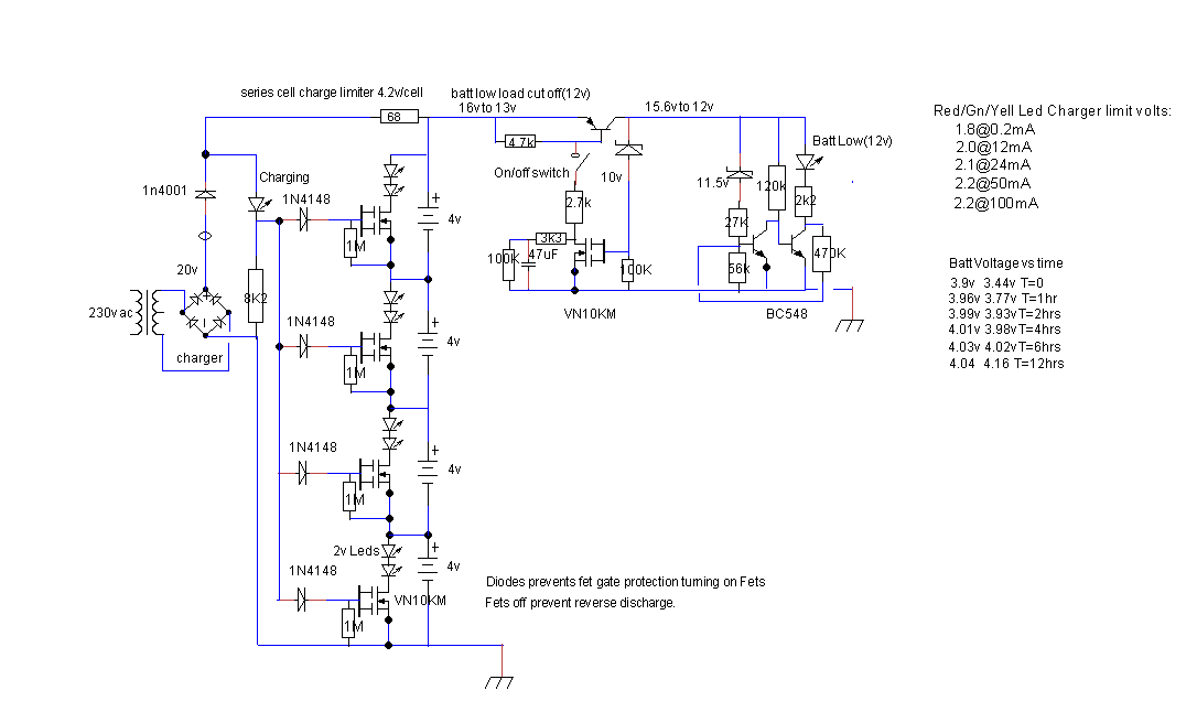
Four 4 volt lithium ion batteries in series provide the driving power to a Pulse Induction circuit I have designed & constructed as described below. These have a special charging circuit using 2 volt Leds to by pass excess current to guarantee each cell will charge to the same voltage. Without this the cells can become unbalanced and eventually lead to cell failure.
Cells charged to a level exceeding the recommended limit will dominate weaker cells & eventually after several charge cycles the weak cells may have no charge while stronger cells have excess charges leading to failure or explosion. Charge control is mandatory for Li Ion cells. Letting cells discharge to zero charge will also cause damage and may cause the cells to ‘go to sleep’ (see batteryuniversity.com) and so if the cell voltages fall below about 3 volts the batteries are disconnected from the load automatically.
The circuit includes Fet devices which switch on to bypass charging curent around the individual batteries. This only happens if the charger current source is applied and crucially if the battery has approached its voltage limit. I am using two 3mm led's in series to act as a bypass 'zener' which limit the battery voltage to just over 4 volts, one advantage being that you can actually see when bypass is in operation. The Led voltage vs current information is as shown on the circuit, obviously for a high current by pass the devices used will need to be changed or paralled together for greater currents. In addition the circuit supplied by the batteries must not be allowed to discharge to zero so a disconnect circuit & warning Led is included.
2) A Pulse Induction Metal Detector Circuit.
Pulse Induction Metal Detector Discussion.
Charge an inductor and its generated field will couple with any metal by virtue of mutual inductance. This coupling affects the ‘Q’ of the inductance so that when the magnetic field is terminated by cutting off the current, the decay of that field is altered by that conductors within that field. Q is the ratio of energy stored to energy dissipated.
Depending on the speed of current cut off, a voltage will be generated, the back emf, which may be several hundreds of volts ( ie E= –L di/dt ). This, together with the capacitance in the circuit, will cause the coil to ring at a resonant frequency. By dissipating the field coil energy through additional parallel resistors, the ringing can be stopped at the point of critical damping having an inherent Q value of 1.
It follows that the Q of the coil will be further changed by any mutual inductively coupled metal within the coil field. Detecting this change in Q caused by metal within the coil field is the job of the detector electronic circuitry.
One way is to measure the amplitude of the back emf with and without metal in the magnetic field. Any energy transferred from coil to metal within the magnetic field will change the Q and also the back emf amplitude. A second method would be to integrate the whole back emf pulse which will show the changed value when the Q is altered.
A third method is to measure the residual current at a point near complete field decay or rather measure the decay delay at a particular current level. The circuit shown does that & also allows for an adjustment for measurements made at extended decayed levels, where the residual coil currents are much lower. By measuring the point where the coil has reduced to a particular current level, the time taken for the back emf to decay to this is measurable ( in microseconds). This time taken will change according to metals detected. Any conductive metals such as gold, aluminium or copper within the field will have drawn energy from the coil thus altering the Q and changing the decay time by a very small amount.
Coil Performance.
A resonant circuit without resistance will only be limited in amplitude by circuit losses. Losses caused by coil resistance and inductive coupling to adjacent metals will de Q the circuit. Further, adding parallel resistance across the coil to dissipate coil energy will tend to mask out inductively couple metals taking energy from the circuit.
If the coil is in a circular configuration the field will be do-nut shaped as the lines of flux form perpendicular to the windings. A coil of 400uH charged to 2 amps and switched off in say 1 uSec will generate some 800 volts of back emf. Without any circuit losses this would resonate with circuit capacitances for a long time. The electronics could count these resonant cycles over a specific period & use it as a measure of circuit Q. Energy taken would change the quantity of cycles present during the period.
Adding any damping resistors will need to stand this voltage so a pair of equivalent series resistors should be used to keep the resistor voltages within spec. Also, the windings need to withstand the voltage, especially if the start & finish run adjacent to each other. A major dump of energy occurs if the switching transistor has a voltage limiter for protection of the switching device.
Increasing the natural resonant frequency of the coil will help to speed up the point where measurements can be made but mostly this is governed by the switching circuit. Damping still needs to be applied for a critically damped coil which needs an oscilloscope to confirm.
The dilemma is to try to keep damping as insignificant as possible so that de Q of the circuit by external metals drawing energy does not get masked by the energy being lost due to added damping or any switching transistor protection. A coil resonating at 1 Mhz would take about a half uSec to reach zero as compared to 1 uSec for 0.5 Mhz. In addition, reducing the back emf with critical damping increases this time to about 4 uSecs or longer. Inductively induced currents occur only when the field is changing, as the coil discharges the transfer of energy slows.
At coil switch off, the enrgy stored in the field collapses and field change is very rapid producing the maximum energy transfer to detectable metals. Detecting must begin as soon after the coil switch of as possible. Once the flux has ceased to change no further energy transfer can take place. Any de Q of the circuit caused by energy transfer can now be measured as the coil voltage aproaches zero.
Discrimination of metals.
In the unlikely event of a non magnetic metal & a magnetic metal are within the same field, then these could cancel any discrimination possibility. Although they would take energy from the coil, any de Q of the circuitry may not produce a measurable time shift. Such a conflict would mean the possibility of missing these detectable metals unless steps are also taken by alternative circuitry to measure the back emf peak voltages which should confirm such a presence.
Increasing the Q of the coil by a magnetic coupled induction will cause a changed time shift as the field pattern becomes concentrated. Decreasing the Q of the circuit with a none magnetic metal will reduce the time shift from its nominal timed delay.
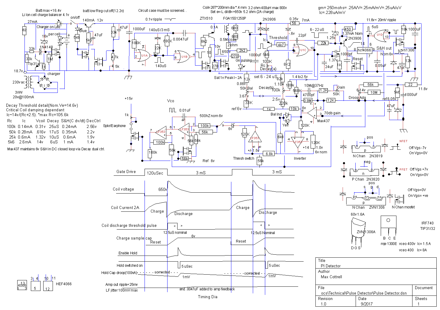
The circuit:
Components used were mainly from stock accumulated over a lifetime so there is an interesting mixture. No processors have been used in the construction. The only reason for using a processor might be to measure the pulse time delay but this can be done by analogue means. The outputs will be flashing lights and audio via connector.
The circuit is pretty conventional & no way unique using an astable gate clock configuration for the timing. Coil charging uses an FGA15S1250P Fet switch with Fet drivers ensuring switch on & off are well controlled. This transistor has a 1250 volt breakdown & can drive many amps if needed, it’s a bit overkill but should not need to dump energy to protect itself. Damping is bled off via bi directional diodes and also an emitter driven pulse detector which has an adjustable collector load. The signal is passed via a logic gate to provide edge sharpening for the sample & hold circuit. This is followed by a high gain amplifier feeding an output multi led display and audio output switch.
Controls.
The time delay control is a 100K pot which acts as the collector load for the pulse delay. This allows a measure of control over the signal threshold depending on the final coil damping current. Any changes to the threshold over its 6 to 24 uSec range needs to be accommodated by the S&H circuit. Feedback from the amplifier is used to maintain the output amplifier balance point by using a long time delay to compensate for any drift. There is aproximately 30 seconds delay before the tracking loop finds its balance. Finally, an amplifier gain control provides up to 70dBs for sensitive searching.
Output Noise
Sources would include coil pick up, clock jitter & sample & hold deviations. A 1 mV deviation at the op amp input will produce a 2.75 volt output deviation which is adequate for driving the balance Led outputs. Further noise reduction is applied to this signal to reduce S & H droop. Any further amplifier feedback may cause oscillation due to the time delay of the sample & hold circuit and auto balance feedback correction.
Performance
This is extremely difficult to quantify because of a number of variables. Sweeping the coil very slowly will reduce the sensing of metals because this reduces rate of signal change causing the balancing circuits to cancel imbalances. Faster sweeps cause the coil flux to increase current induction into the target metal. One way to quantify the sensitivity is to suspend an object from a height and dangle a conductive object over the coil and the let it swing like a pendulum while assesing the signal response. Adjustment of the gain and or delay control will give an empirical idea of its sensitivity for a given piece of metal.
Or just simply try it out !..................M.Cottrell.